




You are here : GEMACENHighlights
- Published on November 9, 2026
- PDF version
Ultrasharp light signatures to probe defects in promising new optoelectronic materials
By studying single crystals of a halide perovskite — an emerging family of materials — at very low temperature, scientists at GEMaC have isolated ultrasharp luminescence lines associated with defects in the crystal. Two recent studies, published in The Journal of Physical Chemistry Letters in collaboration with the LuMIn and FOTON laboratories, show that these defects are collectively sensitive to fluctuations of the crystal lattice and that their emission is strongly polarized.
High-performance semiconductors despite their defects
Halide perovskites form a new class of semiconductors with remarkable optoelectronic properties. They are particularly promising for solar energy conversion, low-energy lighting, photodetection and quantum technologies. Their performance rivals that of the best conventional semiconductors, such as silicon, which accounts for the vast majority of commercial solar cells. Yet while the latter require very complex fabrication techniques, halide perovskites are synthesized much more easily and at low cost using solution-based chemical synthesis techniques. This often results in polycrystalline thin films — that is, films composed of a multitude of assembled crystals. These layers contain a large number of crystalline defects.
While crystalline defects generally degrade the performance of optoelectronic materials, halide perovskites are particularly tolerant to the presence of these defects — an unusual characteristic whose origin remains debated. Several proposed mechanisms involve the soft, polar and dynamic crystal lattice of these materials. Defects play a key role in the properties of any semiconductor, but their experimental identification remains difficult in halide perovskites. In the thin films commonly used and studied, their optical signatures overlap and are strongly broadened by the inhomogeneity of the material.
Ultrasharp optical signatures in single crystals
To overcome this difficulty, the GEMaC team turned to MAPbI3 (CH3NH3PbI3) single crystals, a halide perovskite synthesized at the LuMIn laboratory (ENS Paris-Saclay). Their defect density is about one million times lower than in thin films. At 4 K (−269 °C), the crystals are excited by a laser, which in turn causes the crystal to emit light — a phenomenon called photoluminescence. This photoluminescence can then be studied using spectroscopy techniques. The photoluminescence spectra of these crystals reveal extremely sharp emission lines, with widths below 500 µeV (Figure 1). Such a sharp line is the signature of a highly localized emission originating from point defects. At these temperatures, the thermal energy is so low that charge carriers (electrons and holes) remain trapped near the defects, where they recombine by emitting light.
Defects that fluctuate collectively
In a first study [1], the energy of these lines was tracked over time. It fluctuates on time scales on the order of a second, with amplitudes ranging from a few hundred µeV up to the meV. This spectral diffusion phenomenon is usually regarded as the signature of a single emitter, such as an individual molecule or quantum dot. Yet photon statistics measurements reveal no photon antibunching — the signature of an individual emitter that generates photons one by one. The observed emission therefore originates from an ensemble of emitters that fluctuate in concert. Moreover, several lines associated with distinct defects shift synchronously, indicating that these defects are subject to the same source of fluctuations in their local crystalline environment. These results suggest the existence of domains of slow, correlated deformations of the crystal lattice.
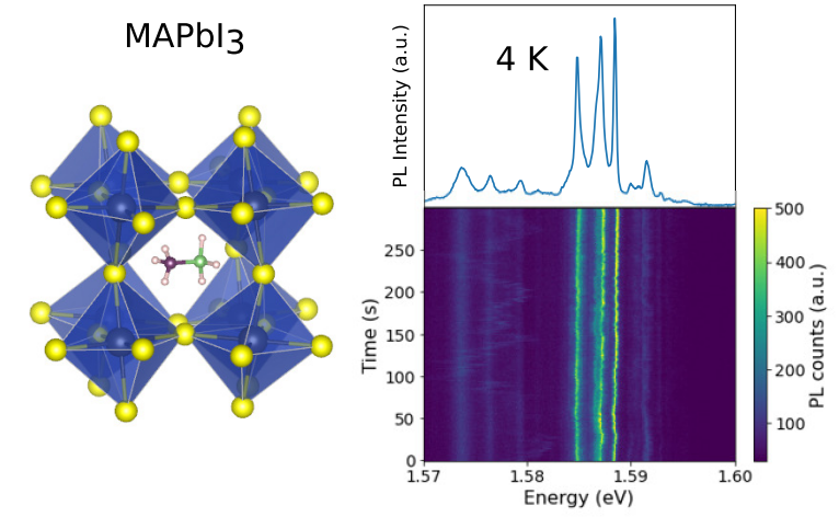
Figure 1. Left, crystal structure of the MAPbI3 perovskite. Right, photoluminescence spectrum of a single crystal at 4 K (−269 °C), showing fine lines associated with defects (top) and the time evolution of this spectrum over 300 s (bottom). The fluctuations of the line energies over time constitute the phenomenon of spectral diffusion.
Polarized emission, excited below the band gap
In a second study [2], these lines were characterized using two complementary techniques. The first, photoluminescence excitation spectroscopy, measures the emitted light intensity as a function of the energy of the laser photons exciting the crystal. The laser energy is scanned around the "band edge", the threshold above which the crystal strongly absorbs light. Just below this threshold, light is absorbed very efficiently, creating free excitons — bound electron–hole pairs. At lower energy, within the band gap, a perfect crystal would be transparent, but defects can still absorb a small part of the light. These measurements show that band-edge excitation, at the free-exciton energy, generates little luminescence from the defect states. In contrast, this defect emission is strongly enhanced when the excitation energy lies slightly below that of the free exciton, about 20 meV below the band edge (Figure 2). This excitation channel is attributed to a transition between a defect level and an energy band.
The second technique, polarization spectroscopy, analyzes the orientation of the electric field of the emitted light, i.e. its polarization. The main observation is that the defect emission is strongly linearly polarized, with a degree of polarization reaching 40%, compared with at most 16% for the band-edge emission. The two emissions have distinct polarization axes. This anisotropy suggests a preferential orientation of the dipoles associated with the defects, imposed by the local symmetry of the emitting centers rather than by that of the crystal. Taken together, these observations are consistent with a hypothesis about the nature of the defect emission: it would arise from an electron passing from one defect to a neighboring defect, a process called donor–acceptor pair recombination.
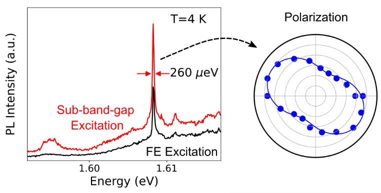
Figure 2. Left, photoluminescence spectra of a defect line (width 260 µeV) at 4 K, under excitation at the free-exciton energy (FE, black) and under sub-band-gap excitation (red). Right, intensity of the line as a function of the polarization analysis angle, revealing strong linear polarization.
Local probes of defect physics
This work, carried out as part of the PhD thesis of Thi Huyen Trang Nguyen at GEMaC, shows that the ultrasharp lines of single crystals make it possible to use defects as sensitive probes of their local environment and of the crystal lattice dynamics. It paves the way for a better understanding of the electronic properties of defects in halide perovskites, a necessary step toward understanding the origin of their defect tolerance.
References
[1] T. H. T. Nguyen, J. M. Urban, A. Delteil, G. Trippé-Allard, E. Deleporte, J. Even, S. Buil, J.-P. Hermier and D. Garrot, “Collective Spectral Diffusion of Defect Luminescence in CH3NH3PbI3 Halide Perovskites”, The Journal of Physical Chemistry Letters 17 (20), 5652–5661 (2026). https://doi.org/10.1021/acs.jpclett.6c00648
[2] T. H. T. Nguyen, G. Trippé-Allard, E. Deleporte and D. Garrot, “Strongly Polarized Emission and Sub-Band-Gap Excitation of Ultrasharp Defect Emitters in MAPbI3 Single Crystals”, The Journal of Physical Chemistry Letters (2026). https://doi.org/10.1021/acs.jpclett.6c02575
Contact
Damien Garrot, GEMaC (damien.garrot@uvsq.fr)
Partners
LuMIn (Laboratoire Lumière, Matière et Interfaces) UMR9024 (Université Paris-Saclay, ENS Paris-Saclay, CNRS, CentraleSupélec).
FOTON (Fonctions Optiques pour les Technologies de l'information) UMR6082 (CNRS, University of Rennes, INSA Rennes).