

You are here : GEMACENResearch teamsAxis 3 – Quantum nanophotonicsNanostructures and colour centres
- Updated on May 22, 2026
- PDF version
Nanostructures and colour centres

This research topic aims at studying the physics of native or artificially induced colour centres in wide gap semiconductor nanostructures and integrating them in devices for quantum technologies.
Colour centres are optically active deep defects, which represent a major interest in quantum information sciences due to their potential as single photon emitters. For instance, NV (nitrogen-vacancy) centres in diamond are at the cornerstone of several major experimental implementations. It has been established during hte last decade that a few other wide gap materials can host colour centres with attractives properties, such as hBN, SiC, ZnO, GaN...
Our research is focused on the study and quantum engineering of colour centres in the 2D material hexagonal boron nitride (hBN). We also consider other material platforms sucha s ZnO and SiC. We focus on structures possessing nanometric dimensions in at least one of the three directions of space (thin layers, nanowires, nanoflakes). They open the way to the realisation of miniaturised devices, integrating optical functionalities (waveguides, optical microcavities, plasmonic resonators) as well as electrical functionalities (contacts for Stark effect).
The research topic is organised into two axes:
- Study of physical properties of native and artificially induced defects
This axis is mainly based on an optical analysis of the fluorescence photon flux (photoluminescence, resonance fluorescence) using spectroscopy, interferometry and photon counting techniques, allowing to access important optical properties with respect to applications in quantum information science (for instance 1st and 2nd order coherence properties, indistinguishability...). We develop specific approaches for the optical investigation of decoherence mechanisms.
- Realisation of integrated devices based on colour centres
Some recent achievements:
- hBN: spatially and spectrally controlled colour centres
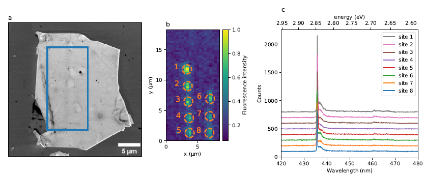
Fig. 1: (a) hBN flake (single crystal of a few tens of nanometres thickness). (b) Confocal photoluminescence map. Eight irradiation sites gave rise to colour centres. (c) Emission spectra of the eight sites, revealing similar emission lines.
Our work has led to the demonstration of indistinguishable photon emission under both non-resonant and resonant laser excitation [4, 12] and laser-based coherent control [5] of the optical transition, opening the way to the use of these emitters for quantum information. Concerning integration, we have demonstrated in-situ monitoring of the emitter creation [3, 14] as well as top-down integration in a monolithic waveguide [6] (figure 2). We have also realised hybrid metal/dielectric planar structures, which have enabled a fundamental study to infer the near-unity quantum efficiency of the emitters, as well as their vertical position in the flake [7].
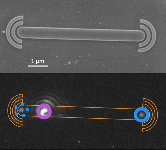
Fig. 2: upper panel: SEM image of a hBN nanofabricated waveguide. Lower panel: photoluminescence of a colour centre subsequently inserted in the structure in a controllable way. The luminescence is guided to the two Bragg couplers at the waveguide output ports.
We are also studying spectral diffusion mechanisms, using an approach based on a combination of resonant laser excitation and photon correlation [5,8,9] and photon correlation Fourier spectroscopy [13]. These approaches makes it possible to identify the type of mechanism (discrete jumps, continuous diffusion) and to characterise it on all time scales.
- ZnO: quantum emitter at the tip of a nanowire.
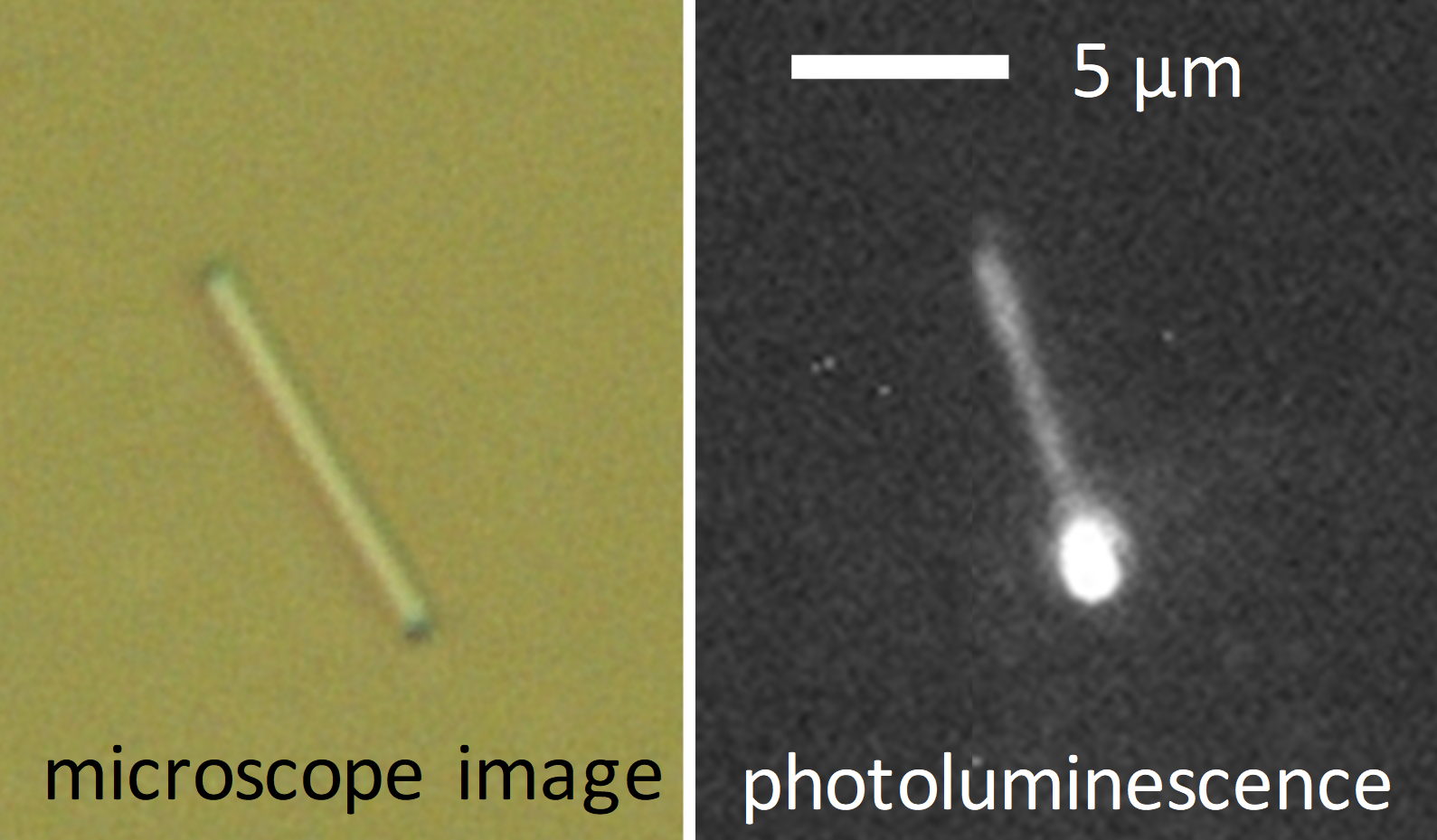
Fig. 2: ZnO nanowire - left: microscope image, right: fluorescence, revealing the presence of a colour centre at its tip.
- SiC: new near infrared optical transitions
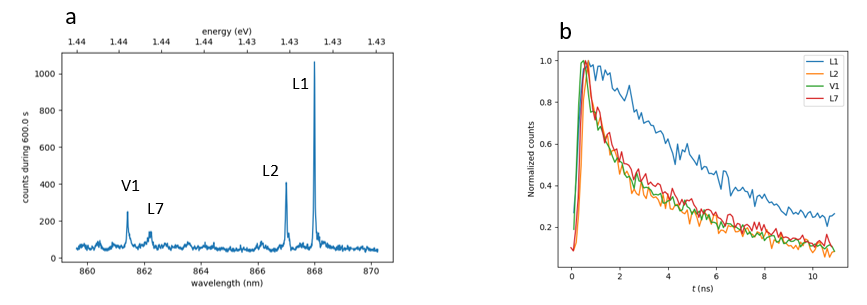
Fig. 3: (a) high resolution spectroscopy of the divacancy in helium-implanted 4H-SiC. The "L-lines" can be observed.
(b) Time-resolved photoluminescence after filtering using a transmission grating, revealing the dynamics and population transfer between the states.
[1] C. Fournier, A. Plaud, S. Roux, A. Pierret, M. Rosticher, K. Watanabe, T. Taniguchi, S. Buil, X. Quélin, J. Barjon, J.-P. Hermier, A. Delteil,
"Position-controlled quantum emitters with reproducible emission wavelength in hexagonal boron nitride",
Nature Communications 12, 3779 (2021) (open access) – [HAL] – [arXiv] – [data]
[2] M. E. Bathen, A. Galeckas, R. Karsthof, A. Delteil, V. Sallet, A. Y. Kuznetsov, L. Vines,
"Resolving Jahn-Teller induced vibronic fine structure of silicon vacancy quantum emission in silicon carbide",
Phys. Rev. B 104, 045120 (2021) – [HAL]
[3] S. Roux, C. Fournier, K. Watanabe, T. Taniguchi, J.-P. Hermier, J. Barjon, A. Delteil,
"Cathodoluminescence monitoring of quantum emitter activation in hexagonal boron nitride",
Appl. Phys. Lett. 121, 184002 (2022) – [HAL] – [arXiv] – [data]
[4] C. Fournier, S. Roux, K. Watanabe, T. Taniguchi, S. Buil, J. Barjon, J.-P. Hermier, A. Delteil,
"Two-photon interference from a quantum emitter in hexagonal boron nitride",
Phys. Rev. Applied 19, L041003 (2023) – [HAL] – [arXiv]
[5] C. Fournier, K. Watanabe, T. Taniguchi, S. Buil, J. Barjon, J.-P. Hermier, A. Delteil,
"Investigating the fast spectral diffusion of a quantum emitter in hBN using resonant excitation and photon correlations",
Phys. Rev. B 107, 195304 (2023) – [HAL] – [arXiv] – [data].
[6] D. Gérard, M. Rosticher, K. Watanabe, T. Taniguchi, J. Barjon, S. Buil, J.-P. Hermier, A. Delteil,
"Top-down integration of a hBN quantum emitter in a monolithic photonic waveguide",
Appl. Phys. Lett. 122, 264001 (2023) – [HAL] – [arXiv] – [data]
[7] D. Gérard, A. Pierret, H. Fartas, B. Bérini, S. Buil, J.-P. Hermier, A. Delteil,
"Quantum efficiency and vertical position of quantum emitters in hBN determined by Purcell effect in hybrid metal-dielectric planar photonic structures",
ACS Photonics 11, 5188 (2024) – [arXiv] – [HAL] – [data]
[8] A. Delteil, S. Buil, J.-P. Hermier,
"Photon statistics of resonantly driven spectrally diffusive quantum emitters",
Phys. Rev. B 109, 155308 (2024) – [HAL] – [arXiv]
[9] D. Gérard, S. Buil, J.-P. Hermier, A. Delteil,
"Crossover from inhomogeneous to homogeneous response of a resonantly driven hBN quantum emitter",
Phys. Rev. B 111, 085304 (2025) – [arXiv] – [HAL]
[10] O. Capelle, G. Amiri, C. Sartel, S. Hassani, A. Lusson, J.-P. Hermier, S. Buil, V. Sallet, A. Delteil,
"Red and infrared colour centres in zinc oxide epitaxial nanowires",
Nanotechnology 36, 245001 (2025) – [HAL] – [data]
[11] H. Fartas, S. Hassani, J.-P. Hermier, N. D. Lai, S. Buil, A. Delteil,
"Reproducible generation of green-emitting color centers in hBN using oxygen annealing",
Appl. Phys. Lett. 127, 014001 (2025) – [HAL] – [arXiv] – [data]
[12] D. Gérard, S. Buil, K. Watanabe, T. Taniguchi, J.-P. Hermier, A. Delteil,
"Resonance fluorescence and indistinguishable photons from a coherently driven B centre in hBN",
Nature Communications 17, 1843 (2026) – [HAL] – [arXiv] - [data]
[13] A. Delteil, S. Buil, J.-P. Hermier,
"Photon correlation Fourier spectroscopy of a B center in hBN",
Phys. Rev. B 113, 125308 (2026) – [HAL] – [arXiv]– [data]
[14] A. Nuñez Marcos, C. Arnold, J. Barjon, S. Buil, J.-P. Hermier, A. Delteil,
"Deterministic generation of single B centers in hBN by one-to-one conversion from UV centers",
ACS Nano 20, 10404 (2026) – [HAL] – [arXiv] – [data]
Contact
Axis 3 – Quantum nanophotonics
Research topics
Members
Permanent staff:
Stéphanie Buil, PR (vice-director of GEMaC)
Jean-Pierre Hermier, PR (head of the team)
Xavier Quélin, PR
Damien Garrot, MCF
Aymeric Delteil, CR
Guillaume Quibeuf, IE
Non permanent staff:
Hien Phan, PhD student
Helmi Fartas, PhD student
Andrés Núñez Marcos, PhD student
Ayoub Gualous, PhD student
Tien Thanh Nguyen, PhD student
Jesús Gómez Sánchez, master student
Former group members