

You are here : GEMACENResearch teamsAxis 3 – Quantum nanophotonicsNear-field optics
- Updated on March 2, 2023
- PDF version
Optical near field: CdSe/CdS single nanocrystal based near-field probe
In the case of the study of a photonic nanostructure, the position of the emitter on the surface must be controlled to account for local fluctuations in the electromagnetic environment. In order to control this position at the nanoscale we have developed an optical near-field probe, falling into the category of active near-field probes, consisting of a single nanocrystal of CdSe/CdS. To realize this nanoprobe we have developed a protocol to graft a single NC at the end of an optical near-field tip by functionalizing a dielectric tip with polymers containing silane thiol groups.
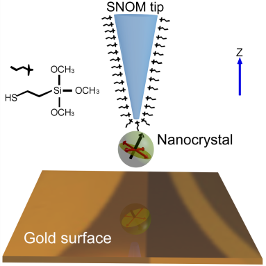
NC hooked to the end of an optical near-field tip
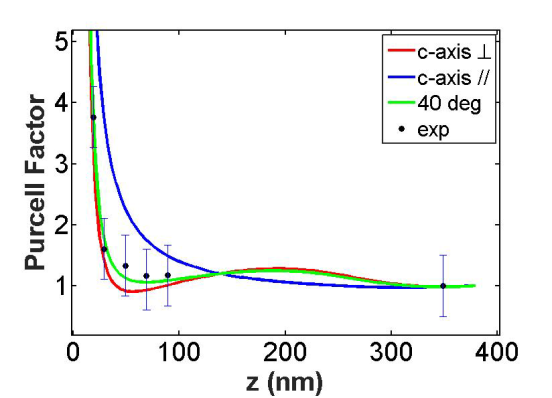
Once the grip has been mastered, the critical point of the NC orientation at the tip remains. Indeed, this orientation is critical if one wishes to probe plasmonic structures afterwards since the interaction of the emitter with the structure is highly dependent on the structure. To determine it, we carry out measurements of the Purcell factor (ratio of the emission rate to the structure to the emission rate to air) for different altitudes on a continuous gold layer of defined thickness. These measurements are compared to a modeling taking into account the polymer layer on the tip. This study is carried out in collaboration with Gérard Colas Des Francs of the LICB (University of Burgundy) and allows us to trace the orientation of different NCx at the tip with an accuracy of a few degrees.
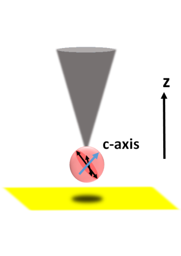
Determination of the orientation of an NC at the SNON tip end, here there is an angle of 40° between the C-axis and the vertical axis.
Once the orientation of the NC has been determined, this tip can be used as a Local Optical State Density Sensor (LDOS). The analysis of the same surface with peaks of different orientation allows to trace the variations of partial LDOS in the 3 directions of space. An example is given here on an array of nanometric holes in a gold layer. The LDOS is probed at different points of the sample and for different orientations of a NC. This study allowed us to show the importance of the variations along the Oz axis (vertical) at a few nanometers from the surface.
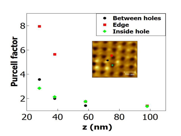
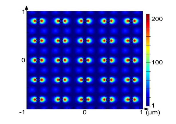
Measurements of Purcell factors at different points on the sample with a tip so the NC has a strong vertical component of the dipole moment. This study is compared to the changes in the vertical component of the electric field calculated in FDTD.
Contact
Axis 3 – Quantum nanophotonics
Research topics
Members
Permanent staff:
Stéphanie Buil, PR (vice-director of GEMaC)
Jean-Pierre Hermier, PR (head of the team)
Xavier Quélin, PR
Damien Garrot, MCF
Aymeric Delteil, CR
Guillaume Quibeuf, IE
Non permanent staff:
Hien Phan, PhD student
Helmi Fartas, PhD student
Andrés Núñez Marcos, PhD student
Ayoub Gualous, PhD student
Tien Thanh Nguyen, PhD student
Jesús Gómez Sánchez, master student
Former group members