

You are here : GEMACENResearch teamsAxis 1 - Semiconductors2D semiconductors
- Updated on June 3, 2025
- PDF version
2D semiconductors
The research activity on boron nitride materials has been carried out in the DIAM team since 2006. Like diamond, hexagonal boron nitride hBN has a wide band gap (6.25 eV) but is part of the 2D semiconductor family whose original properties were highlighted in 2010 shortly after graphene discovery.
Excitons
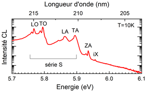
Cathodoluminescence spectrum of the free exciton in hBN
At the European level, the team was asked to join the Graphene Flagship project in 2018 for developing optical characterizations of the 2D materials synthesized in Europe. The aim is to exploit graphene in industrial scale components.
Highly sensitive to their environment, the atomic layers give the best of their optoelectronic properties in devices when they are sandwiched in hBN crystals. The van der Walls heterostructures are the subject of intense research worldwide, extending the physics of semiconductor quantum wells by offering new degrees of freedom in the interactions between atomic layers. At the heart of these stacks currently being studied in the laboratory, hBN alternates with graphene, transition metal dichalcogenides (e.g. MoS2) or black phosphorus (BP).
Axis 1 – Semiconductors
Research topics
Membres
Permanent staff:
Julien Barjon, PRJean-Michel Chauveau, PR
Marie-Amandine Pinault-Thaury, CR
Thierry Kociniewski, MCF
Alain Lusson, CR, directeur du GEMaC
Vincent Sallet, CR
Joseph Scola, MCF
Ingrid Stenger, MCF
Gaelle Amiri, IR
Rémi Gillet, IE
Said Hassani, IR
Corinne Sartel, IR
Non permanent staff:
Sahar Gaddour, PhD studentGeorges Guy Ndamkou Yonkeu, PhD student
Mohammad Abbuayyash, master student