

You are here : GEMACENFacilitiesCharacterisationAFM
- Updated on February 26, 2020
- PDF version
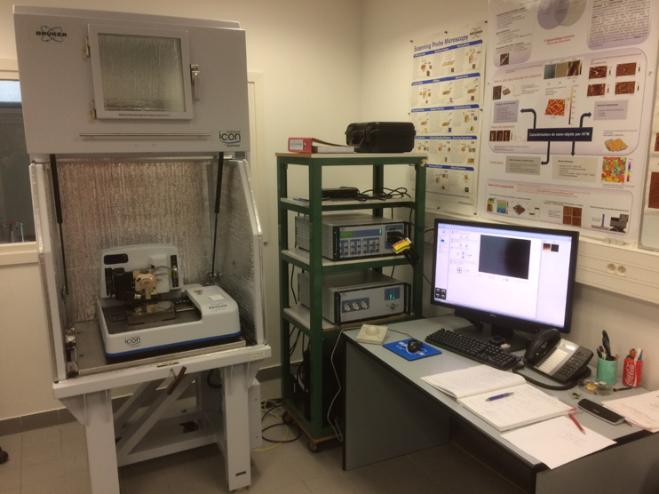
Atomic force microscopy (AFM)
GEMaC has a Bruker Dimension ICON® atomic force microscope, equipped with automatic imaging opticmisation (ScanAsyst ®) in PeakForce tapping mode.
Atomic Force Microscopy is based on the detection of the interactions forces between a probe and a surface of conducting or instulating sample or insulator. The lateral and vertical displacement of the tip above the sample is driven by a piezoelectric tube allowing to characterise the sample surface (roughness) as well as metrologic measurements at the nanometer scale.
3 modes are available: contact mode, tapping and peakForce.
Measurements of the distribution of thelectrical and magnetical gradients (EFM and MFM) are possible, as well as an electrical characterisation (C-AFM module) on samples that are weakly conducting (current range 2 pA to 1 µA).
Manipulation of nano-objects (indentation, local anodic oxidation, etc.) is facilitated by teh Nanolithography software. Measurements can be realised in air or in liquid media. A mapping of the nanomechanical properties is allowed by the QNM® (quantitative nano-mechanical mapping) software, on a large variety of samples (range from 1 MPa to 50 GPa for the Young modulus, and 10 pN to 10 µN for adhesive forces).
Contact
Reservation
Access the online planning