

You are here : GEMACENHighlights
- Published on September 17, 2021
- PDF version
A material conducts to a bright future
GEMaC researchers show how the conductivity of the spinel material ZnGa2O4 can be controlled over a very wide range, opening up applications in ultra-high power electronics and deep ultraviolet optoelectronics.
Spinels form a class of semiconductor crystals with the general formula A B2 X4, where X is usually an oxygen atom O. Among them, zinc gallate (ZnGa2O4) has an ultra-wide band gap (~5 eV). This makes it possible to envisage applications in deep ultraviolet optoelectronics and ultra-high power electronics... provided, however, that we can understand and control its electrical conductivity.
Researchers in GEMaC were able to demonstrate the very high conductivity (3.2 ×10⁻² Ω.cm−1) of an n-type ZnGa2O4 layer. Additional studies to establish the origin of this conductivity were carried out in partnership with collaborators from Yang Ming Chiao Tung National University (Taiwan), the ILV (Institut Lavoisier de Versailles), Da-Yeh University (Taiwan), the ICN2 (Catalan Institute of Nanoscience and Nanotechnology, Barcelona, Spain) and the Horiba company.
This work has provided, for the first time, a fundamental understanding of this high conductivity: in the ZnGa2O4 layer, zinc atoms have strong bond with oxygen atoms, which leads to Zn-O hybridisation. As a result, an impurity band is created which allows electron transport by means of tunneling and hopping.
Spectroscopic and transport measurement techniques were also applied to a p-type zinc gallate layer, synthesised at GEMaC using the vapour phase epitaxy technique. It appears that the type (n or p) of conductivity can be well controlled by adjusting the growth conditions (pressure, oxygen flow rate, cation ratio). The conductivity can be adjusted in a range of more than 10 orders of magnitude. This control of conductivity, which is required for realising devices, clearly confirms the advantages of ZnGa2O4 for power electronics and ultraviolet optoelectronics.
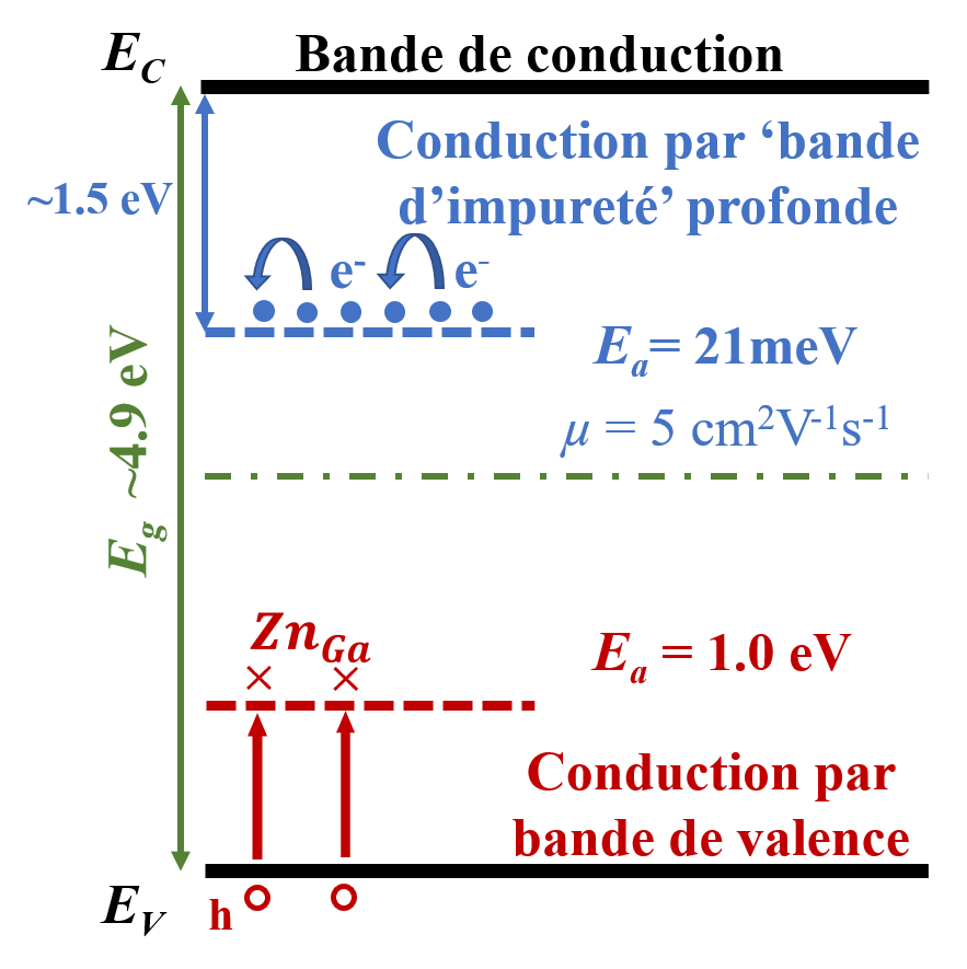
Figure: left: band diagram depicting the conduction mechanisms in n-type ZnGa2O4 (variable range or nearest-neighbour hopping) via the impurity band generated by Zn-O hybridisation, and in p-type ZnGa2O4 (through valance band antisite defects). Right: carrier concentration in n-ZnGa2O4 from 80 to 300 K (top) and in p-ZnGa2O4 from 450 to 850 K (bottom) measured using Hall effect.
Reference:
Z.Chi, F.-G. Tarntair, M. Frégnaux, W.-Y. Wu, C. Sartel, I. Madaci, P. Chapon, V. Sallet, Y.Dumont, A.Pérez-Tomás, R.H. Horng, E. Chikoidze,
"Bipolar self-doping in ultra-wide bandgap spinel ZnGa2O4",
Material Today Physics 20, 100466 (2021)
Contact:
Ekaterina Chikoidze