

You are here : GEMACENHighlights
- Updated on October 20, 2022
- PDF version
A promising material for power electronics and optoelectronics in the ultraviolet range
For the first time, researchers have succeeded in manufacturing large-diameter substrates of both "n" and "p" type β-Ga2O3 semiconductors, making it possible to envision the development of components for both power electronics and optoelectronics in the far ultraviolet.
Gallium oxide is a very promising semiconductor material for power electronics due to its high breakdown voltage. In addition, it has a wide bandgap (> 4.8 eV), which makes it transparent in the ultraviolet range and therefore particularly interesting for the realization of optoelectronic components in this wavelength range (around 250nm). Finally, it has a low manufacturing cost compared to carbon silicide. Today, its main limitation lies in its low thermal properties. But the stakes of such a material are such that many teams around the world are working hard on the understanding of its properties and their improvement. Until now, all the produced gallium oxide-based electronic components were unipolar (only "n" type). However, the first essential step in the manufacture of electronic components involves the creation of bipolar junctions, for which "p" type doping is required.
The feasibility of such a component has just been demonstrated by broad international collaboration, including a team from the Groupe d'étude de la matière condensée (CNRS/UVSQ). Large-diameter pseudo-substrates of β-Ga2O3 on sapphire were manufactured by a French company and then analyzed by GEMaC physicists. They demonstrated the existence of a p-type conduction by Hall and Seebeck effects. These results were supplemented by spectroscopic work and theoretically modelled by other members of the consortium. The results of the study are published in the journal Materials Today Physics.
Through both theoretical and experimental work, the researchers have demonstrated that it is becoming feasible to fabricate p-n bipolar junctions that can withstand higher stresses than Schottky unipolar junctions. In addition, such junctions pave the way for the manufacture of conductive and transparent electrodes, or sensors operating in the far ultraviolet.
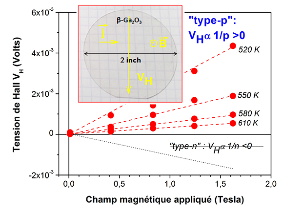
Measurements of Hall voltages as a function of the applied magnetic field at 520 K, 550 K, 580 K, and 610 K, demonstrating "p-type" conduction. The inset shows the 2-inch pseudo-substrate of transparent β-Ga2O3 and the geometry of the measurement: current j, applied magnetic field B, and Hall voltage VH.
For further information, see :
E. Chikoidze et al.,
"P-type β-gallium oxide: A new perspective for power and optoelectronic devices",
Materials Today Physics 3, 118 (2017).
Contact :
Ekaterina Chikoidze