

You are here : GEMACENResearch teamsAxis 1 - Semiconductors
- Partager cette page :
- PDF version
Axis 1 – Semiconductors
Presentation
The research axis 1 Semiconductors aims to develop and study the physical properties of materials, microstructures and nanostructures based on II-VI semiconductors (in particular ZnO, ZnS... ), functional oxides (SrTiO3, LaNiO3), hybrid perovskites for solar applications (CH3NH3Pb(I,Br)3 and Ruddlesden-Popper compounds), as well as the physics of defects in diamond for its applications in electronics, and the study of two-dimensional materials such as hexagonal boron nitride.
In this perspective, we are developing the epitaxial and characterisation processes and techniques necessary for our programmes. We are initiating partnerships, both within GEMaC and with external laboratories, in order to enhance the value of our materials and strengthen our expertise in optical measurements and structural characterisation.
The scientific project of the Semiconductor axis is oriented on the following themes
- Synthesis of diamond in thin layers in order to control its electrical conductivity. The synthesis is associated with an optical spectroscopy activity with techniques dedicated to the study of doping.
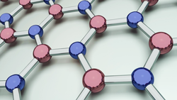
- Study of boron nitride since 2006. The interest of this 2D semiconductor for graphene-based electronic components has emerged since then.
- Nanostructures based on II-VI semiconductors: epitaxy and MOCVD growth mechanisms, study of the doping of ZnO nanowires, lateral or axial complex nano- and heterostructures.
- Optical properties and light emission of 2D and 3D hybrid perovskites for optoelectronics, semiconductors, and quantum structures. This theme covers the study of defects and impurities in semiconductors and nanostructures, quantum confinement, the confined Stark effect, and the effect of constraints.
- Elaboration and functionalization of oxide films. Surface and interface properties are explored: field effect, charge transfer, electric or magnetic polarisation, bi-axial mechanical stress, lifting of orbital degeneracy, chemical reactions in solid phase. In collaboration with the FOX team, this theme includes an activity on epitaxy by atomic layer deposition (ALD, ALE) of functional perovskite oxides such as SrTiO3 and BiFeO3, as well as the elaboration by MOCVD of Ga2O3 films for power electronics.
The team participates in the animation of the scientific community around its themes: GDR PULSE, GDR HPERO, GDR MEETICC, semiconductor nanowires community. We are involved in the training of undergraduate and graduate students from L3 to Master 2, doctoral students, and in teaching courses.

Diamond
Well-known for its brilliance as a gemstone, diamond is also a semiconductor with an exceptional set of physical properties. In its pure state, diamond remains electrically insulating at very high temperatures due to its very wide band gap (5.47 eV indirect). It dissipates heat efficiently thanks to its exceptional thermal conductivity (5 times that of copper) and withstands very high voltages (breakdown field >10 MV/cm). In addition, it has high mobility charge carriers (> 3000 cm2/Vs for electrons and holes). These assets make diamond currently considered as the ultimate semiconductor for power electronics.
However, several obstacles still need to be overcome in order to exploit the full potential of diamond in electronics. The control of electrical conductivity through the addition of impurities (doping) is a major obstacle to the development of diamond electronics. The manufacture of thin diamond layers over large surfaces is another.
The DIAM team is working to remove these "material" bottlenecks with researches focused on the physics of defects and impurities. The team's main theme is n-type doping, with the fabrication and study of the physical properties of thin layers of phosphorus-doped diamond.
Axis 1 – Semiconductors
Research topics
Membres
Permanent staff:
Julien Barjon, PRJean-Michel Chauveau, PR
Marie-Amandine Pinault-Thaury, CR
Thierry Kociniewski, MCF
Alain Lusson, CR, directeur du GEMaC
Vincent Sallet, CR
Joseph Scola, MCF
Ingrid Stenger, MCF
Gaelle Amiri, IR
Rémi Gillet, IE
Said Hassani, IR
Corinne Sartel, IR
Non permanent staff:
Sahar Gaddour, PhD student